Camera-based Sensor for Biomarker Detection
CMOS imaging sensor that captures rich, multidimensional color data from chemical substrates. Unlocks spatial analysis, manufacturing quality control, and defect detection that are impossible with a 1D photodiode signal.
Overview
Designed and built a CMOS imaging sensor-based biomarker measurement system that captures rich, multidimensional color data from chemical substrates. This approach unlocks spatial analysis, manufacturing quality control, and defect detection capabilities that are impossible with a 1D photodiode signal.
Problem
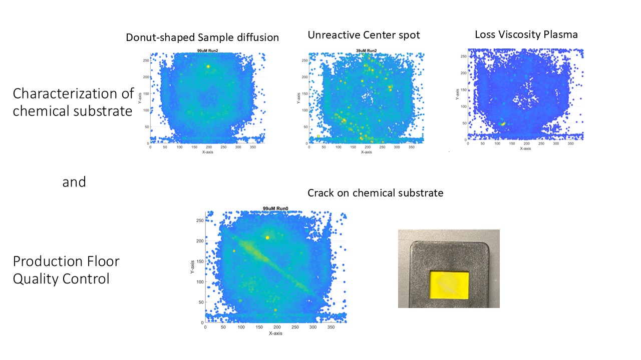
The photodiode solution, while effective, captures only a single voltage value over time. That’s 1D data. This limits the system’s ability to detect substrate-level quality issues such as dust contamination, physical defects, or uneven analyte distribution, all of which directly affect measurement accuracy.
Approach
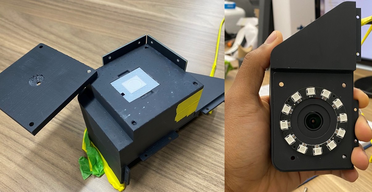
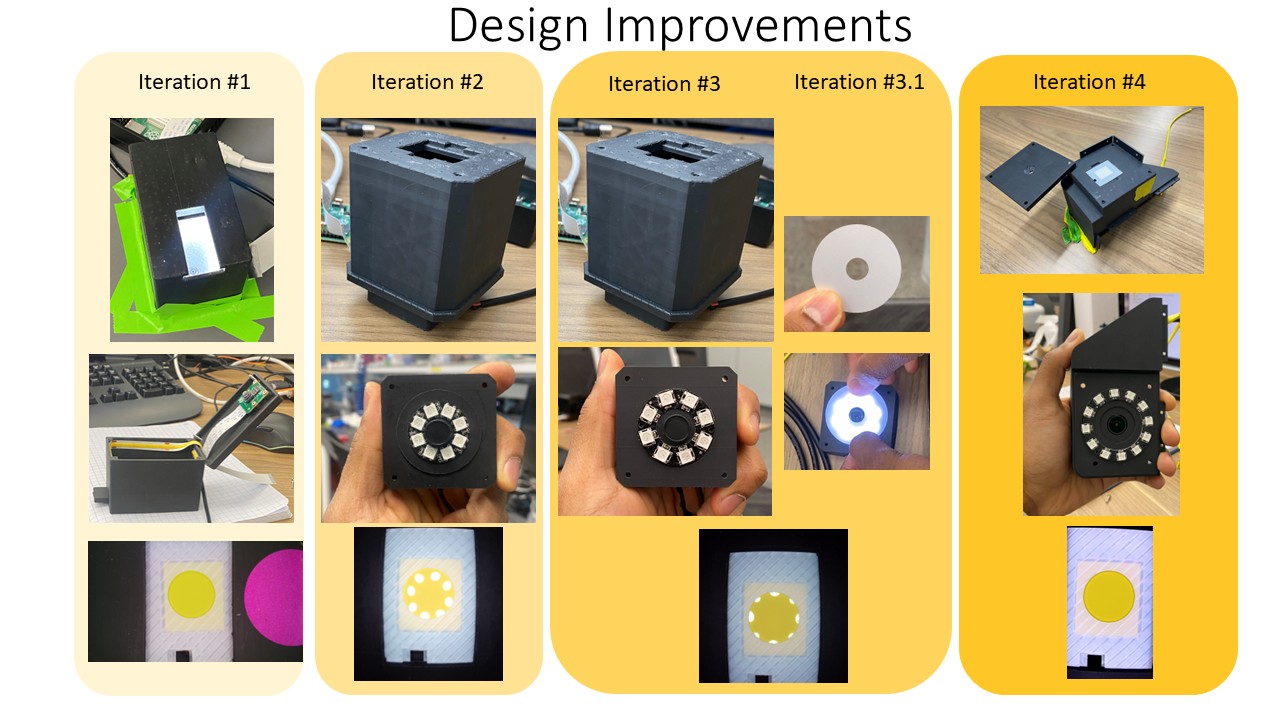
- Iterated through five hardware designs, starting from a GoPro proof-of-concept and ending with a purpose-built system using a 5 MP industrial camera (See3CAM CU55) and a custom 52 mm-radius 12-LED ring.
- Solved critical challenges: disabled auto white-balance to preserve colorimetric fidelity, eliminated bright spots through progressive LED ring scaling, and engineered a sealed 3D-printed chamber with non-reflective lining.
- Tracked RGB pixel values at multiple spatial points on the substrate to map reaction dynamics over time.
Results
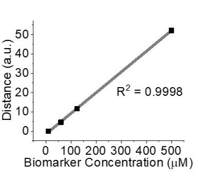
- Captured ~6.2 million data points per image, versus a single voltage reading from the photodiode.
- Reduced background noise to 0.01, 0.27, and 0.45 for R, G, B components respectively, a major improvement over earlier iterations (1.33, 0.92, 1.08).
- Enabled spatial analysis that distinguishes center vs. edge reaction behavior, opening the door to substrate-level quality control and defect detection.
- Maintained the same cost (under $500), compact footprint (15″ × 15″ × 15″), and low power (under 10 W) targets as the photodiode predecessor.
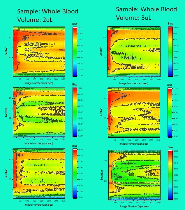
Reaction dynamics
The video below shows the spatial reaction rate captured by the camera, mapped across the substrate. The richness of this signal is what 1D photodiodes can never see.
In use